
During the academic year of 2016-2017 at McMaster University, in conjunction with Dr. DeBruin, Christina Riczu, Thomas Phan and Emilie Corcoran, we developed a compact, battery powered, 12-lead electro-cardiogram. The project won 1st place in the biomedical category at the ECE Capstone Poster Day.
The final report we handed in for the course is attached at the end of this post and includes background information, a design overview, schematics and bill of materials for the hardware we developed. This post will introduce the project and serve as a personal account of the considerations and problems associated with the portion of the project that I focused on.
Before we begin I should note that if you decide to replicate this design or develop a derived design that you are doing so at your own risk. Attaching a device with a low impedance connection to a person can be dangerous. We developed this project under a supervisor with experience developing and maintaining such devices and protocols were put into place to ensure safety.
System Design
My goal during the project was to develop the most compact device possible while providing robust mechanical design, usable battery life, convenient connectivity, a clean user interface, and good analog performance. For this to occur components must be selected carefully across electrical, mechanical and software domains. In addition to this I wanted the design to be reusable and extendable in the future, choices were made to allow the circuit boards to be used for different applications beyond this project.
Overview
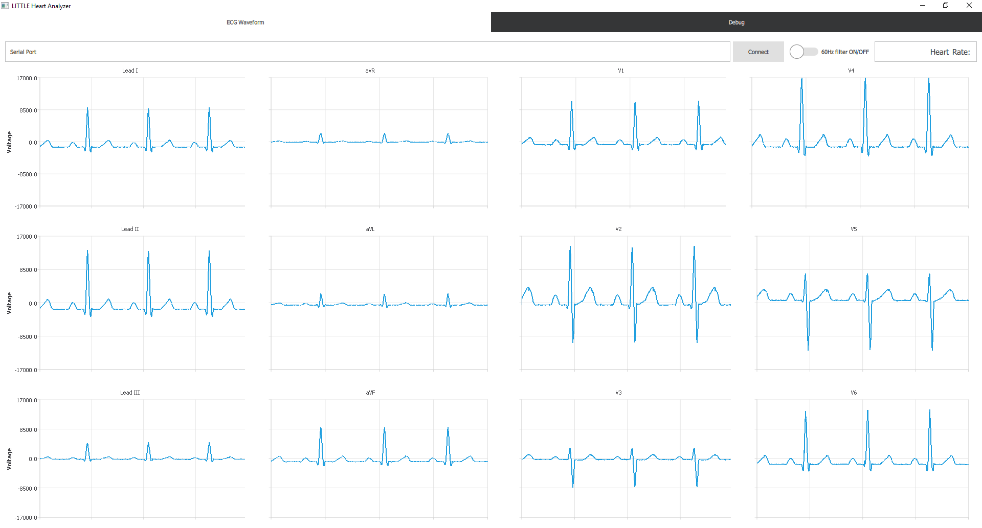
The purpose of the hardware is to perform signal conditioning, analog to digital conversion and transfer the data to a host.
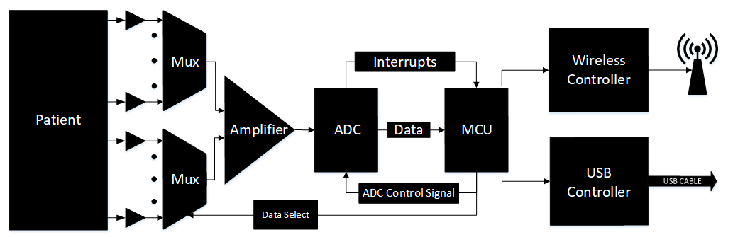
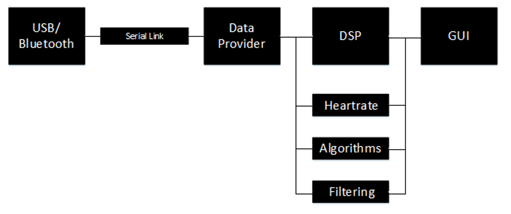
The software processes the data and displays it in a graphical interface.
Patient Interface
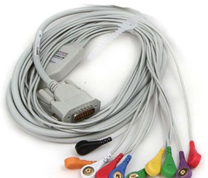
Low cost cables for connecting skin electrodes to a data acquisition system is available on EBay. If you search for Contec ECG cable on EBay you will find them for about $20. They interface with a DB15 connector and come terminated with button snap connectors for connecting with commonly available ECG electrodes such as the 3M Red Dot silver-silver chloride electrodes.
We could not find a pin out for the cable so we used a continuity meter to figure it out, I include it here in case anyone needs it.
| Pin | Electrode |
| 1 | V2 |
| 2 | V3 |
| 3 | V4 |
| 4 | V5 |
| 5 | V6 |
| 6 | Shield |
| 7 | Not Connected |
| 8 | Not Connected |
| 9 | Right Arm |
| 10 | Left Arm |
| 11 | Left Leg |
| 12 | V1 |
| 13 | Not Connected |
| 14 | Right Leg |
| 15 | Not Connected |
Electrical
We begin with electrical component selection as this dictates the direction we must go for mechanical and firmware integration.
Isolated Power
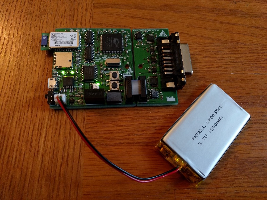
As mentioned before, electrical isolation is required for safety. Batteries can be used to provide a simple isolated supply, however, requiring the replacement of batteries puts an unnecessary burden on the user. We wanted the device to be convenient which meant we wanted the device to be battery powered and rechargeable even during use. This necessitated an isolated DCDC converter between the battery and electronics connected to the patient for safety.
The system was developed to allow the DCDC converter to be sized smaller thus allowing the device to fit into a smaller box. From the top-level schematics, you can see that some components are powered by the battery through a 3.3V linear regulator and only the components with a direct connection to the patient is powered by the isolated DCDC.


The use of a switching converter to power an analog front end meant that we need some noise filtering. The ROE-3.305S isolated DCDC converter we are using comes from RECOM’s Econoline series of switching converters that are designed to be small but it outputs a lot of ripple because the designers did not include a lot of output filtering. A common mode choke will cut down on any common mode noise generated by the isolated DCDC and the LC output filter will filter out much of the switching transients generated by the 80 kHz switching frequency of the ROE-3.305S. The LC backfeed filter is the filter recommended by RECOM to pass some EMC compliance standard test, no calculations were performed by us for backfeed filter.
The result is an analog front end working with signals that have an amplitude of a few millivolts being powered from a switching converter with no noticeable noise issues.
The Bluetooth module and MicroSD card requiring higher currents at 3.3V were powered through the linear regulator by the lithium polymer cell. USB power is provided to a charging circuit on this side of isolation as well. On the other side of isolation, we have the microcontroller with analog to digital converters and connection to the analog front end which contains our operational amplifiers, instrumentation amplifiers, analog multiplexers, and analog buffers all powered at 5V to allow for a larger input range at our analog input. The microcontroller and analog front end do not consume much power compared to the Bluetooth radio and MicroSD card allowing us to size our isolated DCDC converter for up to 200 mA current draw at the output. This was critical as it allowed our system to fit into a smaller box due to height constraints.
Microcontroller Selection
The choice of which microcontroller to use was based on IO mapping flexibility and elimination of external peripherals. The Cypress PSoC5LP was chosen because each pin is remappable making circuit board routing easier resulting in a more compact circuit board and the integrated analog to digital converters supported variable full-scale input range and level shifting. This was key to allow for the use of a multiplexed switched front end to eliminate components in the analog front end. The ease, flexibility and configurability all the digital and analog peripherals implemented using fixed function blocks and universal digital blocks enables the creation of an elegant data acquisition system.
Analog Front End
The analog front end was developed to be compact, we chose to create a multiplexed switched front end to reduce component count, however this means we cannot use high pass filters for removing DC offset, low pass filters to remove out of band noise or notch filters to remove power line noise. This imposed challenges we tackled in the digital domain using the microcontroller we chose earlier. This resulted in a compact analog front end that was not much bigger then the patient lead connector itself.

All components on the analog front end were chosen to be low noise, support rail to rail operating and be small in size.
An Linear Technology LT1920 is used as the instrumentation amplifier, this is however unnecessary since a high input impedance is not required at this stage. It was used because it uses a single resistor to set the gain and we already had this part on hand from making single lead ECGs using it.
Resistors in this schematic do not have values specified, the resistor values were chosen later.
Communications
For communications to the host system we incorporated Bluetooth connectivity and USB connectivity. Having both allows us to communicate both with PCs that do not have Bluetooth connectivity and Android devices which almost all have Bluetooth connectivity.
The Bluetooth module was placed in such a way that the antenna hangs off the board and sits in free air away from the aluminum enclosure to maintain good range. The resulting system demonstrated excellent range of about 25 meters through a cinderblock wall.
Mechanical
Low cost aluminum boxes are available from Digikey. An aluminum box allowed our device to be compact and robust against damage.
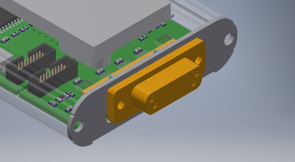
The size of the box was constrained by to a minimum height by the DB15 connector used for the patient lead cable. We used this height as a driving constraint for the selection of the DCDC converter.
As can be seen, the DCDC converter is the tallest component on the circuit board and has about 1 mm of clearance from the top of box.
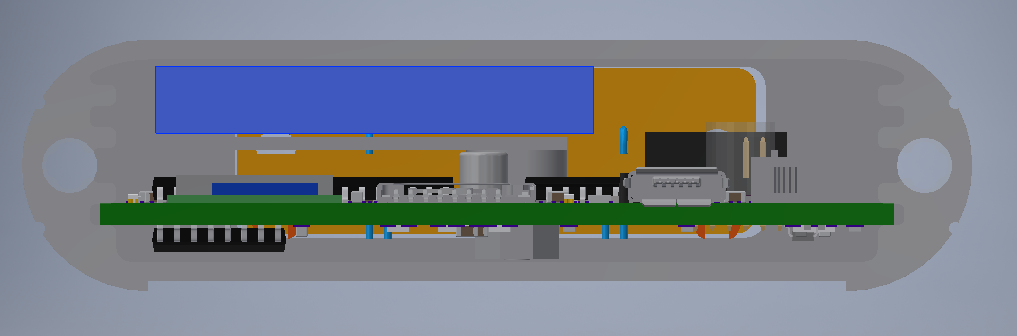
All tall components were placed on one side of the board to make room for the battery and battery tray. The space available became the driving factor for sizing the battery as long as the battery was of high enough capacity, else we would have had to buy a longer box with the same cross-sectional design.
Firmware and Peripheral System
Our firmware was implemented on top of FreeRTOS to allow for future extensibility even though our project did not require an RTOS. A scheduler would allow us to implement on board DSP algorithms in parallel with data sampling and communications easily in the future to allow for processed data to be stored on the MicroSD card which was unused for this project.
The customizable peripheral system with flexible analog components on the PSoC5LP allowed us to use the multiplexed switched analog front end implemented in hardware.
Software
The choice of implementing the user interface and digital signal processing backend in C++ using Qt was made to ensure we could implement both a high-performance backend and fluid user interface.
Qt also provides methods for inter-thread communication and this enables ease of running digital signal processing routines in parallel allowing for the system to be extended in the future.
A bonus for using Qt is that the same code and interface can be used for desktop and mobile platforms. The use of Qt Quick allows the creation of touch and mouse friendly interfaces with ease.
Design Challenges
Analog Multiplexer Charge Injection
Initially we wanted to reduce the cost of the analog front end by feeding the electrode signals directly into the analog multiplexers and use the LT1920 instrumentation amplifier similar to the way it is normally used, connected directly to the electrode pair. Unfortunately, it turns out that when analog multiplexers switch, even those designed to inject only a small amount of charge when switching will still result in a significant voltage transient when coupled with the high input impedance of the instrumentation amplifier and the lack of ability of the human body to dissipate even a few nanocoulombs of charge.
This waveform of a switching transient with a 5 uS settling time was captured with a breadboard prototype hooked up to a patient simulator. A 5 uS settling time would not be a problem as it would limit our sample rate to 200 kHz, however it turned out that the patient simulator had much lower output impedance and ability to dissipate charge verses an actual human body. We never captured the waveform of a switching transient with the multiplexer hooked up to one of us but it was awful.
To fix this we added unity gain buffers before the analog multiplexers and that fixed our problems.
Analog Sampling System with DC Offset Cancellation
Our design challenges for the analog sampling system begin at the analog front end, the decision to design a switched front end imposes some requirements on the data acquisition system.
The skin/electrode interface creates a half cell potential, or a DC offset that can be up to a few hundred millivolts and is unmatched between electrode pairs. Since we are unable to use analog filters in the analog front end as their settling times will be much too long when switching we are unable to remove this DC component using high pass filters. This means the instrumentation amplifier which amplifies differential voltages will apply gain to the DC offset. Resulting in a signal that can easily clip effectively removing all the interesting AC components in the signal. To avoid this, we must limit the gain on the instrumentation amplifier necessitating a small full-scale range on the ADC performing the sampling.
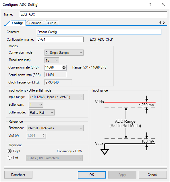
We configured the instrumentation amplifier for a gain of 25x, with an input amplitude of up to +/- 5mV this resulted in a signal of +/- 125 mV. The ADC on the Cypress PSoC5LP was configured for an input range of +/- 128 mV. Unfortunately, this presents another problem, because the DC offset in the incoming signal is unknown the ADC can now easily clip. We decided to remedy this situation with the use of another ADC with a low resolution and high input range allowing us to sample the DC offset of the incoming signal. We then set the negative reference terminal of the high resolution low input range ADC to the DC offset using a DAC. The DC offset is sampled and the DAC is driven with a new value in sync with the switching of the analog multiplexer.
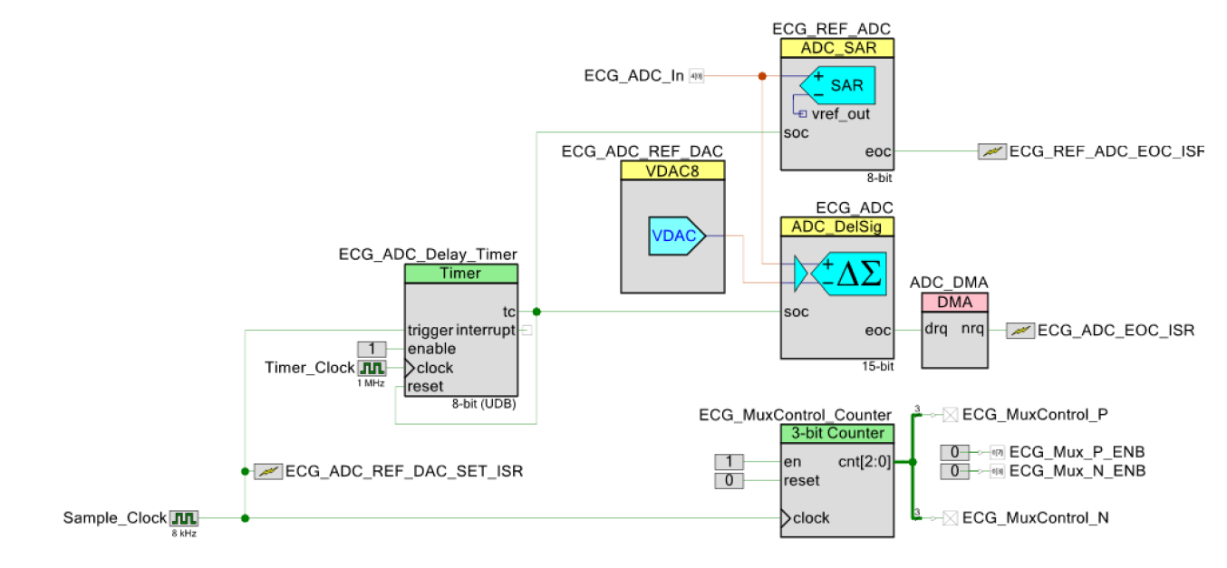
We have 8 channels to sample so the Sample_Clock running at 8 kHz will result in a 1 kHz sample rate per channel, the ECG signal has a bandwidth of about 200 Hz, we over-sample here because we have no low pass filters to prevent aliasing.
The ECG_ADC_REF_DAC_SET_ISR will fire at the same time the ECG_MuxControl_Counter is triggered. This sets the ECG_ADC_REF_DAC to the time-averaged DC offset measured previously by the ECG_REF_ADC which has an input range of 0 to 4.096V at 8 bits of resolution and changes the channel being fed into the ECG_ADC_In analog input pin connected to the output of the analog multiplexers on the analog front end. The ECG_ADC_REF_DAC voltage is fed into the negative input of the ECG_ADC effectively shifting its operating voltage range to the expected DC offset for the channel.
The ECG_ADC_Delay_Timer is used to delay sampling by the two ADCs until the DAC and any remaining switching transients have settled. Values from the ECG_REF_ADC is read out by an interrupt service routine, the rolling average of voltages for each channel is stored for use by the ECG_ADC_REF_DAC. The ECG_ADC uses a DMA for data transfer to keep CPU load low.
This system effectively performs DC offset cancellation and analog data acquisition, since the DAC is only 8 bits when the DC offset changes a step can be seen in the output waveform but this could be compensated in software and the data can then be passed through a digital high pass filter to remove all DC offset but this was not implemented in our code.
USB Data Transfer
Bluetooth data transfer worked without a hitch with the Bluetooth module in Serial Port Protocol mode where it emulates a COM port on the host system. USB data transfer did not work quite as well at first.
It turns out that the USB CDC driver only fires a single event in Qt for each USB bulk transfer that occurs to reduce the number of event handlers being invoked. To maximize our data transfer rate 64 1 byte values are transferred per bulk transfer. This means we must handle the data in blocks. We decided to frame our data into 515 byte frames, 512 bytes of data or 64 samples per channel and a 3 byte header. The header is 0xFF, 0xFF, 0xDA. 0xFFFF is an impossible ADC value because our ADC is configured for 15 bits so it acts as our sync word, 0xDA stands for DATA allowing us to use other headers for commands from the device to host or side channel data for DC offset reporting that would allow us to remove the artifacts in the data introduced by the DAC’s large voltage steps.
Another necessary routine in the data receiver in the host application was detection of loss of sync and a fast method of finding the sync word again if any data is dropped. A loop is used to consume data quickly and find the header without exiting the event handler and synchronization is regained resulting in a sampling artifact too small to see in the output data.
Final Report
Attached below is a copy of our final report and appendices containing background information, a design overview, our presentation materials, schematics, bill of materials, pictures and connector pin-outs.
Little Heart Analyzer – Final Report
Sources and Design Files
Circuit board designs were created in CircuitMaker and is available here.
Software sources were created for Qt Creator and PSoC Creator and is available here.
hi i’m jihoon lee from korea
i study the ECG module without analog filter like your research and read this report
so, i tested using instrumentation amplifier INA128 and LT1920 with same circuit design as yours
but both chips didn’t operate in gain of 25x(used resistor is 2 Kohm), reference 2.4V, and sine wave(30hz, input range 5mV~50mV, offset 0V)
however, when i applied offset voltage of sine wave about 1.1V~1.3V, signal shown in oscilloscope(wave min: 2.8V, max:3.5, input voltage 50mV)
is this normal? does this circuit need to input the offset voltage with the aforementioned that?
if you have time, please you answer me how i set the design and test environments
i’ll be looking forward to your reply
thank you
Hi Jihoon,
You should need an offset voltage applied to the input waveform close to the same as the reference voltage. That is expected, the patient will have the reference voltage applied to them through the RL drive terminal.
oh..
I missed RL drive voltage to be applied to the body
your research and this reply helped me greatly
Thank you once again!!
Hi!!
Congrats!! very interesting your methodology. But I have some doubts:
1.- Where’s the driven leg circuit?
2.- What voltage reference do you use at your INA LT1920?
Thanks in advance.
Hi, sorry for the late reply.
Both the right leg drive circuit and voltage reference is directly driven by DACs internally in the PSoC5LP microcontroller, the voltages are set and never changed even though we can change them in software. This may not be the most accurate and low noise approach but seems to work well regardless since the absolute voltage does not actually matter that much (DC offset from the electrodes is much larger then any voltage error we have), no significant noise is visible in the waveform after data capture so that seems to be a non-issue as well.
The right leg drive is not the typical noise cancellation feedback circuit you sometimes find in references, that technique is actually not necessary with newer instrumentation amps (probably anything made in the last 20 years really…). The circuit was proposed in an early application note to increase the common mode rejection ratio, a value that was low in old instrumentation amp designs but is very high in the LT1920 we used.
Hi can i ask you question i hope you can answer me. If i want to find the equation of the 6 lead ECG which they are (lead1, lead2,lead 3, aVR, aVL and aVF) by using a multiplexer and an instrumentation amplifier do you know how i can do that
because really i tried to find the solution but it’s rally hard i hope you can help me
Hi Nada, the lead derivation is done in our source code. https://github.com/AlexLao512/Little_Heart_Analyzer/blob/master/Software/Qt_Creator/ECG_DSP.cpp
It should also be in our project report attached at the end of this article.
I would really love to use this ecg design in my dissertation for creating a low-cost fully integrated system that can take ecg signals and then use machine learning to tell if the person is suffering from myocardial infarction. However Altium has a bug where you can’t access the full pcb files in circuitmaker anymore. Could you please attach the files in a mega or dropbox? it would be much appreciated
Hey Pierse, What kind of problem are you having? I installed the CircuitMaker desktop application and can open the files no problem. I unfortunately do not see any way to export the actual files, they seem to be locked into the cloud for this free Altium tool.
Hi Alex, Whenever I try to open the files from the CircuitMaker website I get a pop-up saying that I need the CircuitMaker application installed to open the file (which I have installed already) then when I tried opening the files in Altium 365 and selecting open with CircuitMaker it will open the application but won’t actually open the project. There’s a couple people talking about this bug on the CircuitMaker Forum so I don’t think it’s just me. If possible could you share read-only access with me through Altium 365 as I think this should resolve the problem, my email is piersechapman@gmail.com. Thank you very much for your time
I think I shared it, let me know if that works.